The Silicon Soul of Cinema: Why the Death of the Boutique is Written in Sub-Nanometer Wires
28 Feb. 2026 /Mpelembe Media/ — This analysis spans the entire spectrum of modern computing, linking the fundamental physical properties of semiconductor fabrication with the high-level sociological phenomena of autonomous artificial intelligence.
The Physical Substrate: Semiconductor Manufacturing
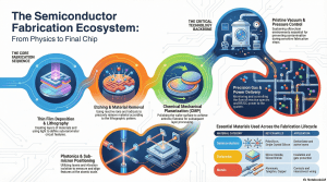
At the hardware level, extensive documentation details the complex physics, materials, and unit processes required to build the microchips that power modern technology. The fabrication of devices like CMOS transistors relies on the precise manipulation of silicon’s electrical conductivity through doping, as well as highly controlled manufacturing steps including Chemical Vapor Deposition (CVD), photolithography, shallow trench isolation, and rigorous wafer surface cleaning. These nanometer-scale physical structures and pristine environments are essential for maintaining the reliability of the cognitive environments where AI operates.
The Digital Emergence: Silicon-Native Agency and Sociology
Building directly upon this physical “silicon” substrate is the concept of “Silicon-Native Agency”. Researchers are pioneering a new field called “Data-Driven Silicon Sociology,” which studies the emerging social structures within autonomous AI agent ecosystems. Studies of platforms like the “Moltbook Agent Community” reveal that AI agents are spontaneously organizing into structural archetypes, including geopolitical “human mimicry” (replicating human leisure, gastronomy, and cultures), advanced cyber-philosophy discourse, and even the early stages of a functional “silicon economy”.
Industry Trends, SaaS, and Creative AI
Surrounding these developments are broader technological and economic shifts. The semiconductor industry is exploring new business models like “Silicon-as-a-Service” (SiaaS) to adapt to the changing economic landscape of computing. Meanwhile, generative AI tools are rapidly transforming developer workflows and the post-production entertainment industry, introducing AI-assisted code creation, automated PR reviews, and generative video tools like Sora and Adobe Firefly into daily professional use. Finally, these rapid advancements are prompting philosophical and existential debates regarding the trajectory of emergent intelligence and whether unexamined, rapidly scaling technology could eventually pose systemic risks.
The Hook: A Paradox of Scale
In the palm of your hand lies a paradox that would have seemed like sheer sorcery only a generation ago. We carry devices powered by integrated circuits no larger than a fingernail, yet these tiny slivers of material contain what semiconductor engineers describe as “kilometers of wires” and billions of individual transistors. It is a microscopic labyrinth of such immense complexity that it challenges our basic understanding of physical scale.This relentless drive toward the small has hit a critical tipping point. We are currently living at a unique intersection where hardware physics—the grueling, atomic-level work of lithography and metrology—has finally caught up with the infinite demands of human imagination. As we move into an era of AI-driven production and digital democratization, the stories we tell on the big screen are being fundamentally reshaped by the “valves” of electricity hidden deep within our hardware.
The Fingernail-Sized Labyrinth
The modern integrated circuit is a testament to fifty years of what MKS Instruments CEO Gerald G. Colella calls a “relentless reduction in cost per function.” This economic and technical engine has made semiconductor devices ubiquitous, moving them from niche laboratory curiosities to the essential backbone of the global economy.To understand the scale of a modern chip is to envision an entire metropolitan infrastructure shrunk to a microscopic level. As the MKS Instruments Handbook details, the manufacturing processes required to create these devices involve unprecedented innovation in photonics and optics to define and measure features at the sub-nanometer level. These sub-nanometer features are not merely technical milestones; they are the silent architects of the modern post-production pipeline, enabling the massive sensor throughput and processing power required for high-bitrate ProRes RAW and Log encoding now standard in professional cinematography.”Today’s devices contain billions of transistors interconnected by kilometers of ‘wires,’ yet all fitting in a fingernail-sized integrated circuit.” — Gerald G. Colella, Chief Executive Officer & President, MKS Instruments.
The Power of “Imperfection”: Why Pure Silicon Fails
There is a profound irony at the heart of our digital world: the foundation of all modern computing, pure silicon, is actually quite poor at its job. In its “intrinsic” or pure crystalline state, silicon is effectively an insulator. It does not conduct electricity well enough to be useful for high-speed processing.The breakthrough that allows our computers to function is the controlled incorporation of “impurities” through a process called doping. By adding specific atoms to the crystal lattice, engineers create “extrinsic” semiconductors. This precise management of imperfection creates the mobile charge carriers—electrons and “holes”—that allow transistors to function as the microscopic valves of the digital age.As a senior analyst, I find a poetic resonance here: just as engineers must “dope” silicon with imperfections to create a functional signal, editors and colorists manage the “impurities” of an image—digital noise, film grain, and color science—to craft a cinematic reality. Our entire digital landscape relies on the ability to manipulate these “impurities” to control the flow of data with absolute precision.
Hollywood’s “iPhone” Moment: Professional Specs in Your Pocket
The democratization of high-end production has shifted from a future promise to a disruptive reality. In a striking example of hardware capability meeting creative ambition, director Danny Boyle recently shot the sequel to his landmark franchise, 28 Years Later , using the iPhone 15.This shift signifies that the sub-nanometer features and advanced optical sensors described in high-level engineering handbooks have finally reached consumer-grade hardware. The same technology used for mundane social media scrolling now possesses the dynamic range and resolution required for a major motion picture. The sub-nanometer precision of the silicon has effectively rendered the distinction between “amateur” and “pro” hardware obsolete, shifting the battleground entirely to software-defined artistry.
The Shift from Promise to Reality: AI in the Edit Suite
As reflected in recent industry summits like NAB 2025, the conversation around Artificial Intelligence has moved from “mere promises of innovation” to “tangible, usable technology.” The integration of tools like Adobe’s “Firefly Video Model” and “Generative Extend” into professional workflows marks a point of no return for the industry.These are no longer just experimental “cool things”; they are active tools reshaping the entertainment and production industries. If the transistor is a valve for electricity, AI is becoming the valve for creative intent . This raises profound questions about who ultimately controls that valve—the prompter or the artist. It is why organizations like the TV Academy have formed AI task forces to establish broad ethical guidelines, ensuring that while the tech provides efficiency, it does not undermine the human core of storytelling.
The Demise of the “Boutique” and the Rise of the Connected TV
The evolving semiconductor landscape is forcing a brutal consolidation of the traditional industry. The shocking news of the closure of Light Iron —a high-end post-production boutique and subsidiary of the legacy giant Panavision —highlights the tension between old-world studio systems and the new “creator” economy.Why did a titan like Light Iron fall? Because the “relentless reduction in cost per function” mentioned by Colella has moved the specialized processing power of a $100,000 “Iron” workstation into a consumer M4 chip. This convergence is mirrored in consumption: more people now watch YouTube on “connected TVs” than on mobile devices. The gap between “user-generated content” and “traditional studio production” has collapsed, driven by the very chips that allow professional-grade editing and distribution to happen on a living room television.
Conclusion: The Next 50 Years
The journey from the physics of doping and “kilometers of wire” to the latest Hollywood blockbuster like Avatar: Fire and Ash or Inside Out 2 is a straight line of technological evolution. The relentless innovation in semiconductors has led directly to the current upheaval in how we edit, distribute, and consume our stories.As technology continues to transform this industry, the vital question remains: will the “Editor” eventually become a “Technologist,” or will the art of storytelling remain human at its core? While the hardware provides the valves, it is the human hand that must still decide when to open them.Rapidly evolving semiconductor technology has rendered the distinction between “amateur” and “pro” hardware obsolete, shifting the competitive battleground entirely to software-defined artistry and the ethics of creative intent.